Intel held its Unleashed Webcast yesterday and in the event, Intel CEO Pat Gelsinger unveiled some new details about the Ponte Vecchio Xe-HPC 7nm GPUs. The Ponte Vecchio will be the company’s largest chip that has been designed to date.
The Ponte Vecchio GPU will be making use of several key technologies that were highlighted in yesterday’s event. They will power 47 different compute tiles based on different process nodes and architectures.
Intel Ponte Vecchio is the first and foremost GOU based on the Xe-HPC graphics architecture which is the flagship product leveraging Intel’s 7nm EUV process node. Not only that, the silicon is using many other compute tiles that are based on different process nodes, all of which merge into one singular exascale graphics processing unit known as Ponte Vecchio.

Image Credit: Intel
The Ponte Vecchio GPU will primarily use Intel’s own 7nm EUV process node but it will also be producing some Xe-HPC compute dies through external fabs. There are other tiles that are essential for the Ponte Vecchio GPU to work and those are fabricated on TSMC’s 7nm process node. Raja Koduri teased the use of 7 advanced technologies in the Ponte Vecchio.
Following is what technologies Intel will be utilizing in the Ponte Vecchio GPU as shared by Raja Koduri in a tweet:
- 16 Xe HPC (internal/external)
- 8 Rambo (internal)
- 2 Xe Base (internal)
- 11 EMIB (internal)
- 2 Xe Link (external)
- 8 HBM (external)
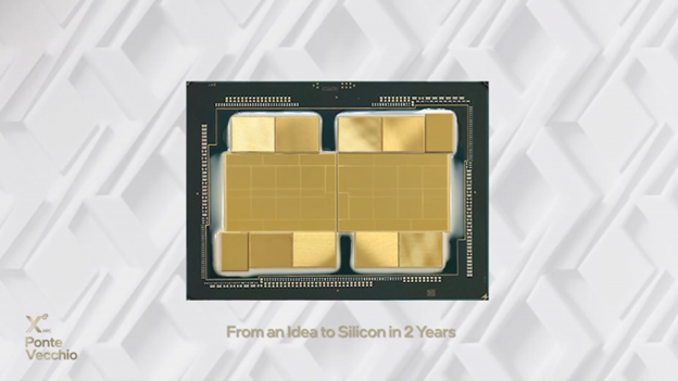
Image Credit: Intel
In the details revealed in the Unleashed Webcast yesterday, Intel described that the Ponte Vecchio chip is actually composed of two separate GPU dies, each consisting of six Xe-HPC Compute units. A pair of these Compute Units are directly attached to a Rambo Cache which utilizes the Intel 10nm Enhanced SuperFin process node.
Each GPU block is also attached to four HBM2 stacks which could either be 4-hi or 8-hi. There are eight HBM2 stacks in total that will offer multi-GBs of memory capacity with loads of bandwidth. There are also 8 passive die stiffeners on each GPU.
The main GPU makes use of Foveros 3D packaging to connect the GPU compute units with the cache while the EMIB interconnects the HBM2 and Xe Link I/O tile with the main GPU. The GPU also makes use of 11 EMIB dies that are featured underneath the HBM2 and I/O link chips. Forveros offers inter-GPU connectivity (GPU + Cache) within the same tiles while EMIB offers connectivity for off-die tiles (HBM2 with GPU).

Image Credit: Intel
For now, it is not known how many EUs the Xe HPC GPUs will have. However, Intel has previously detailed that its Xe HPC GPUs will feature 1000s of EUs. In its Xe LP GPUs, Intel features 8 EUs per subslice. A subslice within a Gen 12 GPU is similar to the NVIDIA SM unit inside the GPC or an AMD CU within the Shader Engine.
Intel currently features 8 EUs per subslice on its Gen 9.5 and Gen 11 GPUs so if the same hierarchy is kept, we can see a significant number of Super-Slices consisting of many subslices.

Image Credit: Intel
Here are the actual EU counts of Intel’s various MCM-based Xe HP GPUs along with estimated core counts and TFLOPs:
- Intel Xe HP (12.5) 1-Tile GPU: 512 EU [Est: 4096 Cores, 12.2 TFLOPs assuming 1.5GHz, 150W]
- Intel Xe HP (12.5) 2-Tile GPU: 1024 EUs [Est: 8192 Cores, 20.48 assuming 1.25 GHz, TFLOPs, 300W]
- Intel Xe HP (12.5) 4-Tile GPU: 2048 EUs [Est: 16,384 Cores, 36 TFLOPs assuming 1.1 GHz, 400W/500W]
Intel Xe class GPUs would feature variable vector width as mentioned below:
- SIMT (GPU Style)
- SIMD (CPU Style)
- SIMT + SIMD (Max Performance)
Intel further details the EUs in its conference. The EUs will be connected with a new scalable memory fabric known as XEMF (XE Memory Fabric) to several high-bandwidth memory channels. The Xe HPC architecture would also include a very large unified cache known as Rambo cache which would connect several GPUs together.
Intel also announced some new optimization improvements in the 7nm process node. The 7nm process node 2x density scaling vs 10nm, Planned intra-node optimizations, 4x reduction in design rules, EUV and Next-Gen Foveros, and EMIB Packaging.

Image Credit: Intel
Intel has unveiled that the Ponte Vecchio GPUs will be heading out first to the Aurora supercomputer with shipments beginning later this year. The GPU will compete against NVIDIA’s Ada Lovelace and AMD’s cDNA 2 graphics architectures in the HPC segment.